
Bond wireless building blocks provide a new approach to power modules
The Hybrid Electric Vehicle is bringing new challenges and opportunities for power semiconductor packaging, in particular those without bond wires. Here we discuss how using discrete bond wireless building blocks in the CooliR2DIE approach can be used to develop a complete module. By Ben Jackson, Senior Manager, Automotive Power Switch & Power Module Product Management & Business Development, for International Rectifier.
Power density is a phrase often associated with servers and computers, but rarely with respect to cars. This may lead people to think that in fact power density really is not important for a vehicle. But this could not be further from the truth. Take a look under the hood of a modern car and you will see there is barely room to get a wrench in between the tightly packed systems – every bit of space has been used up – the car by its very nature is space constrained and the trend is for smaller and more compact vehicles in order to deliver better fuel efficiency. At the same time the weight of the vehicle is also being more closely scrutinized as, simply put, weight equals fuel! To that end vehicle manufactures now proudly boast how many kilograms they have managed to shave off the car when a new model year is brought out. So given this, why is power density so loosely associated with cars? The answer lies in the incumbent technology, the internal combustion engine. The high energy density of gasoline at about 45MJ/kg means that the internal combustion engine and its belt driven pumps and fans is a very energy-dense solution. Compare this to the energy density of a traditional lead acid battery at about 0.1MJ/kg it is easy to see one obstacle that the new hybrid and electric solutions need to overcome. Of course battery technologies on (H)EVs are now well beyond that of a lead acid battery, but the gap is still large.
The concept of the COOLiR²DIE package, as shown in Figure 1, uses Solderable Front Metal (SFM) technology, which enables the removal of the bond wires usually needed to connect to the silicon. Available as a discrete component the COOLiR²DIE is reflowed down to the substrate, this allows module manufactures to greatly simplify their manufacturing process and indeed system assemblers who had previously not been able to enter the module market to make inroads without the need for expensive die handling and wire bonding equipment. At the same time International Rectifier has taken the COOLiR²DIE technology and constructed a range of transfer molder power modules, COOLiR²MODULE in particular a half bridge module, COOLiR²BRIDGE.
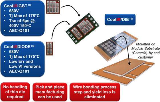
Figure 1: The COOLiR² bond wireless packaging concept
As can be clearly seen in figure 1 the elimination of the bond wires along with the Direct Bonded Copper (DBC) sandwich construction means that there is an electrically isolated surface on both sides of the semiconductor, a surface that can be used for cooling and for adding thermal mass in close proximity to the IGBT and DIODE. Figure 2 gives an example of how the flexible cooling arrangement can be used to increase the current handling capability.
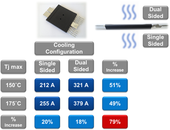
Figure 2: Enhanced current handing capability with dual sided silicon and a maximum junction temperature of 175ºC
In a traditional wire bonded power module commonly found on the market today the system can be cooled from the bottom side, and usually the silicon is limited with a maximum junction temperature of 150ºC. In the example shown in Figure 2 this would enable the module to carry around 212A with a given size of IGBT and DIODE inside. With the COOLiR²BRIDGE (see Figure 2) a second cooling path through the top side of the module can be accommodated. Depending on mechanical construction this presents the possibility of halving the thermal resistance from junction to ambient. In reality about a 50% increase in current can be achieved with the same size of IGBT and DIODE as used in the traditional wire bonded module. Importantly this enables power handling performance to be improved without spending on costly larger IGBTs and DIDOES, and moreover the power density is improved. By virtue of the COOLiRIGBT and COOLiRDIODE silicon inside the module having a Tj maximum of 175ºC it is then possible to increase the rated current of the module by around another 20%. Putting the two features together, the same size of IGBT and DIODE can reach around 380A rather than the 212A in the traditional wire bonded module – almost an 80% improvement!
It is then important to look at the lower half of the equation when it comes to power density; how much space or volume the solution takes up. Figure 3 shows a comparison between a popular 400A wire bonded module and a 480A COOLiR²BRIDGE. By eliminating the wire bonds the form factor is dramatically reduced allowing the current density to increase by a factor of two while the weight for a three-phase solution is reduced by 260g. Next the large SFM connections to the die provide a much lower inductance electrical path, up to a factor of 60% lower at 12nH for the loop inductance of the module. This is a characteristic which translates to various system level benefits; with a lower parasitic inductance the voltage overshoot associated with the switching of high currents can be reduced. This in turn gives the system designer more margin and flexibility while of course the direct benefit of lower inductance, less ringing and smoother switching enabling a more efficient and EMC friendly system to be achieved.
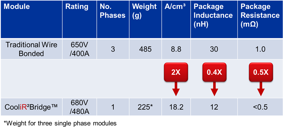
Figure 3: A comparison between a traditional gel-filled module using wire bonds and the bond wireless COOLiR²BRIDGE
Finally consideration should be given to the package resistance, as shown in Figure 3 this is reduced by 50% to under 0.5mΩ. At the low voltage end of the power electronics spectrum a 40V MOSFET with an Rds(on) of 0.5mΩ would be state of the art so it might seem trivial to be highlighting a such a reduction in package resistance on a high voltage system. But it is also critical to remember that the (H)EV main inverter is a high current system, so at a current of 400A a saving of half a milliohm in resistance results in a power saving of 80W, significant for improving efficiency, reducing heat sink size and cooling requirements.
With the high energy density of gasoline and the ability to refuel a car in a matter of minutes it can be argued that energy density and the efficiency of the systems that feed off the internal combustion engine are not of concern. However on an (H)EV with limited and expensive battery capacity, and hours - rather than minutes - required to ‘refill the tank’, it becomes far more important to consider how efficiently we use the energy stored on board the vehicle. Automobiles are considered an established piece of technology, perhaps even an ‘old’ invention, but innovation will be needed at every step to ensure the successful evolution from gasoline to electricity.
Product Spotlight
APV1111GVY
Panasonic

Panasonic PhotoMOS® Photovoltaic MOSFET High-Power Drivers
| SKU: | |
|---|---|
| Stock: | 3490 |
| Cost: | $3.95 |
